【Destructive Analysis】
SEMScanning Electron Microscopy (SEM) is powerful to inspect the surface topography and microstructure of solid samples uses optoelectronic system to focus electrons generated by an electronic gun onto a small spot on the sample surface. This beam of electrons will then interact with the sample material to generate secondary electrons, back scatter and signature X-Ray etc. A scan coil is then placed on sample surface to pick up those signals. The SEM works by collecting secondary electrons to form an image. 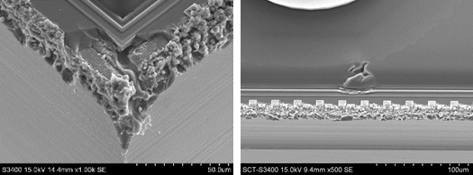
|
|
12” Wafer-Level D-FIBThe 12” Wafer-level dual-beam FIB equipment is capable of simultaneously imaging the cross section by electron beams while cleaving the sample with ion beams. As well as performing the EDX composition analysis. 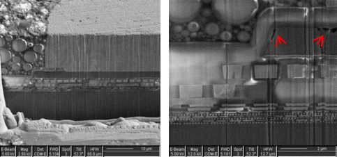
|
|
Cross Section Destructive AnalysisUse the mix glue to fill the sample around to enhance to sample structure to avoid the sample destructive while cross section then using the different type sand paper to process cross section in the specific area (point) or non-specific area (non-point) for observing easily. 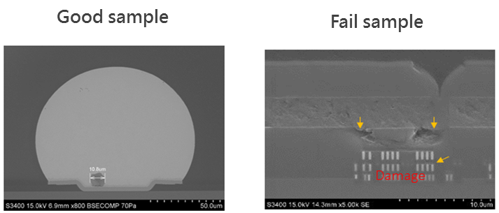
|
Chemical Destructive AnalysisUse chemical de-solution to etching package achieve de-cap, compound removal, die take out or de-solder then inspection chip or device defect issue (ex. wire bond issue, die crack, chipping, Scratch…) 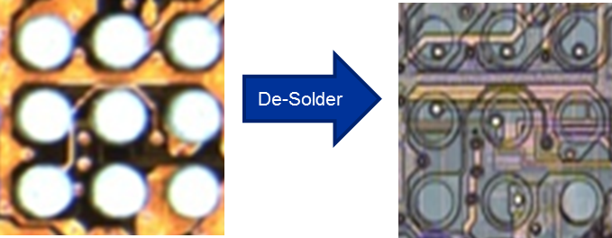
|