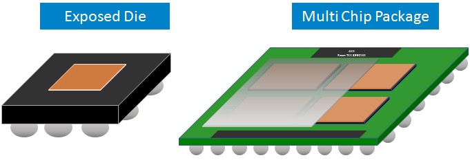
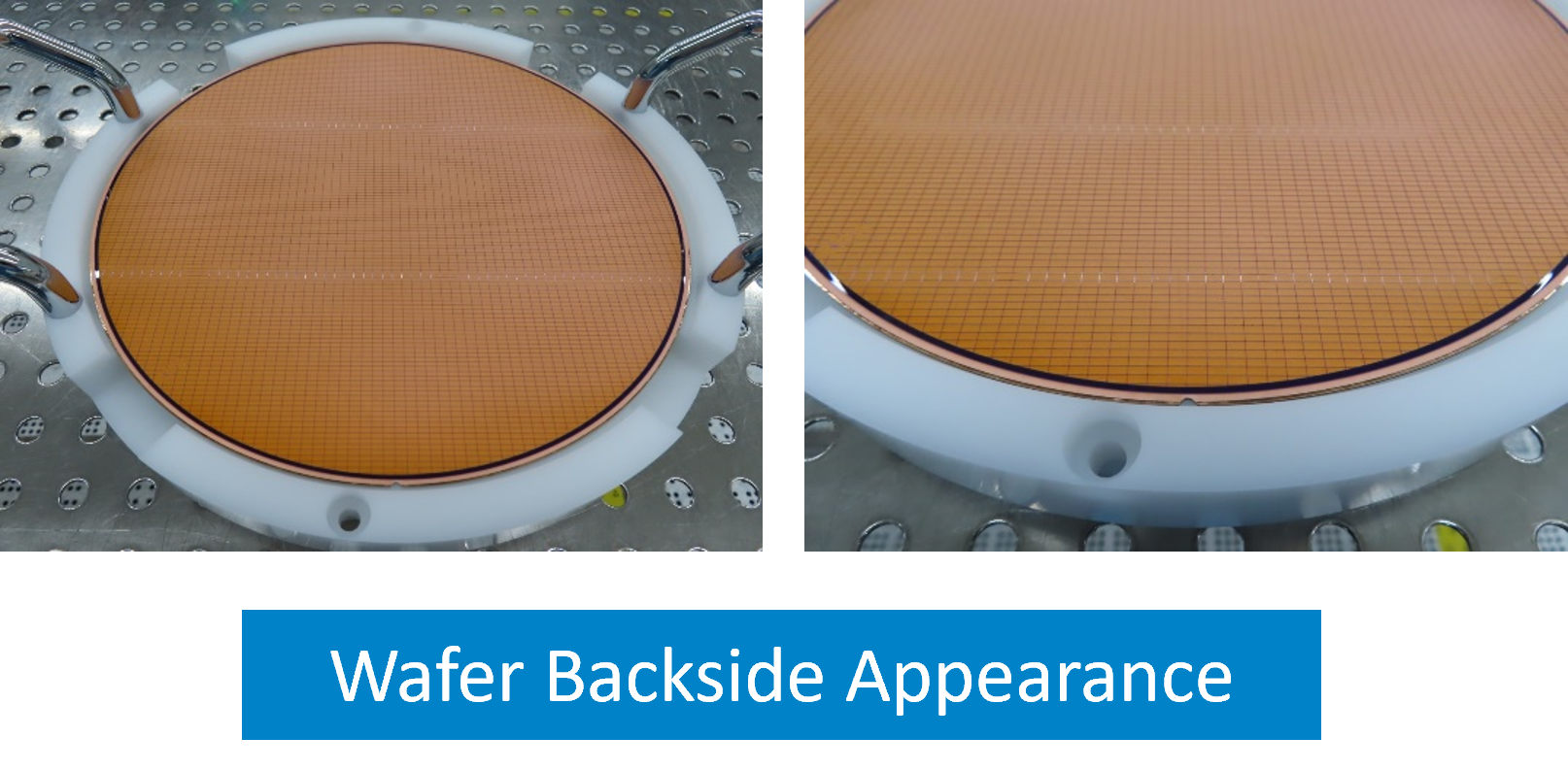
Backside Metallization
High performance computing will generate high volume heat during calculation. Backside metallization are with deposition of metal layers on the bare backside silicon to enhance its thermal conductivity. It provides better thermal efficiency than conventional Epoxy Molded packages.
Applications
PMIC, High Performance Computing, AIoT Edge Computing, Cryptocurrency, Heat Sink, EMI Shield…etc

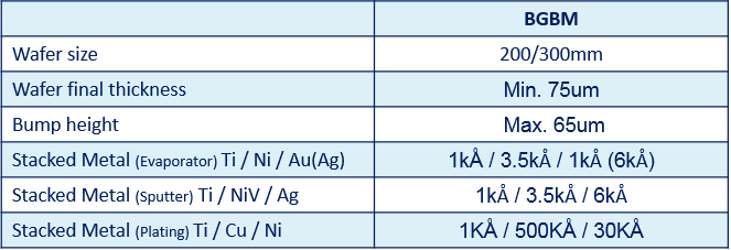
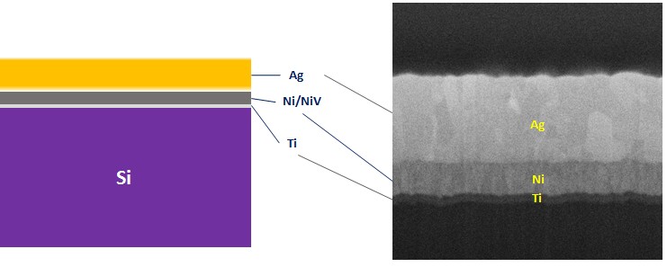
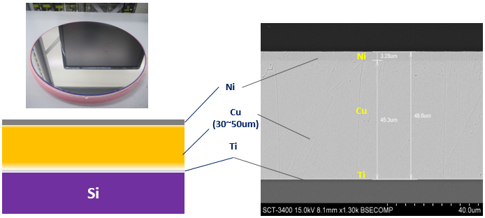
Specifications & Capability
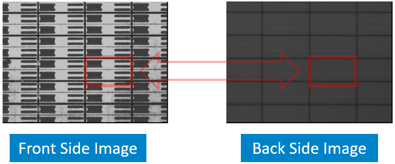
Backside Alignment
To expose the backside patterning align with the frontside circuit pattern, the scribe line will not be covered by metal to cause the poor dicing quality.
Backside Metallization Process Flow