
銅柱無鉛凸塊Cu Pillar Bump
針對高密度與極細腳距(Fine Pitch)封裝需求,提供具備卓越電氣與熱傳導效能的「銅柱無鉛凸塊(Cu Pillar Bump)」技術。此技術能有效克服傳統錫鉛凸塊在微縮過程中的橋接(Bridging)風險,提供極佳的電遷移(Electromigration)抵抗力與高度穩定性。For high-density and fine-pitch packaging requirements, we offer Cu Pillar Bump technology delivering superior electrical and thermal performance. This technology effectively overcomes the bridging risk of conventional solder bumps during scaling, providing excellent electromigration resistance and high reliability.
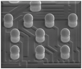
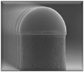
| Item | Specification |
| Wafer Size | 200mm / 300mm |
| Minimum Pitch | ≥ 40 um |
| Solder Composition | Lead-free SnAg |
| Dielectric Material | PI / PBO |
晶圓級晶粒尺寸封裝Wafer Level Chip Scale Package (WLCSP)
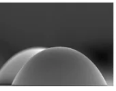
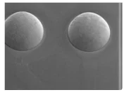
現行封裝方法中,其封裝尺寸為最輕薄短小的類型(最接近晶片原始大小的封裝),絕大多數應用場景為行動裝置及智慧穿戴裝置,可提供植球及電鍍球兩種 WLCSP 製程服務以對應不同應用需求。Among current packaging methods, WLCSP offers the smallest, thinnest form factor — closest to the original die size — and is widely used in mobile and wearable devices. We offer both Ball Drop and Plating Bump WLCSP processes to meet different application needs.
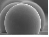
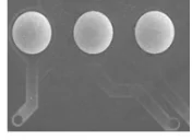
| Item | Specification |
| Wafer Size | 200mm / 300mm |
| I/O Count | < 250 |
| Die Size | 0.2 x 0.4mm ~ 7 x 7mm |
| Bump Pitch | 500um ~ 300um |
| Bump Height | 70um ~ 250um |
| Solder Ball Pitch | ≥ 200um |
| Solder Ball Size | 100um |
| Solder Composition | SnAg1.8% / SAC105 / SAC405 |
結構剖面圖Structure Cross-Section
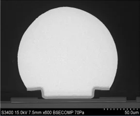
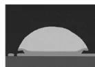
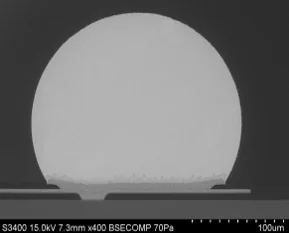
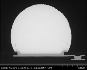
※ 亦提供 2P1M 結構;詳細堆疊規格與客製化方案,歡迎聯繫業務窗口進一步討論。※ 2P1M structure is also available. For detailed stack-up specifications and customized solutions, please contact our sales team.
無鉛銲錫凸塊Lead-Free C4 Bump
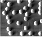
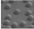
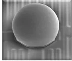
因應環保法規與無鉛化趨勢,提供高可靠度的 C4 無鉛銲錫凸塊技術,廣泛應用於覆晶載板封裝(Flip Chip)及晶圓級晶粒尺寸封裝(WLCSP)。In response to environmental regulations and the lead-free trend, we offer highly reliable C4 Lead-Free Bump technology, widely used in Flip Chip substrate packaging and Wafer Level Chip Scale Packaging (WLCSP).
| Item | Specification |
| Wafer Size | 200mm / 300mm |
| I/O Count | ~ 1,000 |
| Die Size | ≤ 12 x 12mm |
| Bump Pitch | ≥ 150um |
| Bump Height | ≤ 100um |
| Solder Composition | SnAg 1.8% |
| Dielectric Material | PI / PBO |
電鍍凸塊/植球/金屬重佈線層Plating Bump / Ball Drop / RDL
可根據客戶特殊要求訂製,提供產出非標準結構之凸塊服務(例如:WLCSP 電鍍凸塊 – 追求更薄的封裝整體高度)。Customizable to specific customer requirements, offering non-standard bump structures — for example, WLCSP plating bumps engineered for a thinner overall package height.
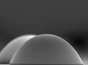
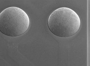
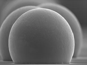
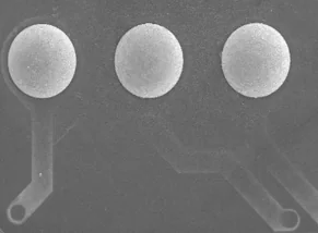
傳統導線架封裝會增加整體封裝尺寸的大小,使用扇入式金屬重佈線層可維持封裝大小與晶粒尺寸相近且可更輕薄小,加上減少了信號傳輸路徑,相較打線封裝類別可以得到更佳的電氣性能。Traditional leadframe packaging increases overall package size. Fan-in RDL keeps the package size close to the die size for a thinner, more compact form factor, and its shorter signal path delivers better electrical performance than wire-bonded packages.
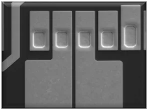
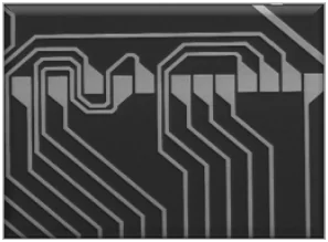
| Cu | |
| RDL Space | ≥ 10 um |
| RDL Width | ≥ 10 um |
| RDL Thickness | ≤ 20 um |
晶背金屬化Backside Metallization (BGBM)
因應高速率運算所產生的熱效應,可利用裸晶背面披覆金屬層的方式來加快其導熱效率,較之傳統的 Epoxy Molded 封裝晶粒其散熱效率有更好的表現。To address the heat generated by high-speed computing, a metal layer is applied to the backside of the bare die to accelerate heat dissipation — delivering better thermal performance than conventional Epoxy Molded packaging.
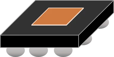
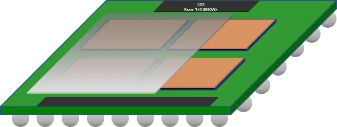
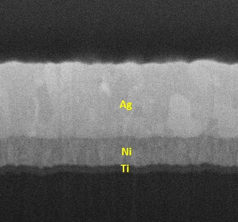
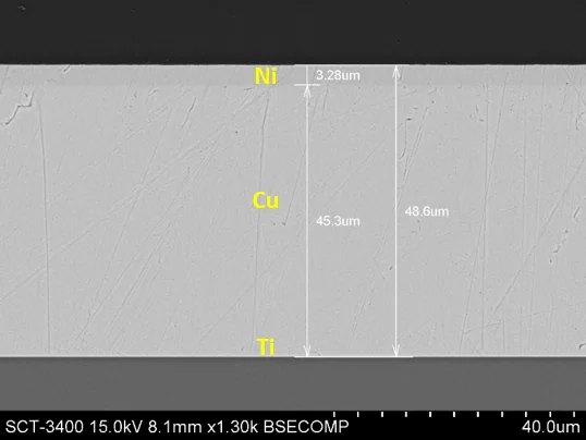
利用晶圓背面黃光製程將背面金屬圖形轉移至晶背,且與正面活動區電路對齊,切割道也可透過該過程去除金屬,已達到更好的切割品質。A backside photolithography process transfers the backside metal pattern onto the die back, aligning it with the front-side active circuit area. This process can also remove metal from the dicing streets, achieving better dicing quality.
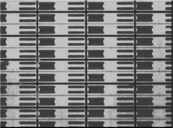
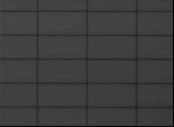
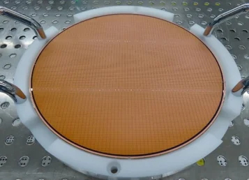
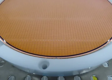
背面金屬化完成外觀Completed Backside Metallization Appearance
| Item | Specification |
| Wafer Size | 200mm / 300mm |
| Wafer Final Thickness | Min. 75 um |
| Bump Height | Max. 65 um |
| Stacked Metal (Evaporator) Ti / Ni / Au(Ag) | 1 kÅ / 3.5 kÅ / 1 kÅ (6 kÅ) |
| Stacked Metal (Sputter) Ti / NiV / Ag | 1 kÅ / 3.5 kÅ / 6 kÅ |
| Stacked Metal (Plating) Ti / Cu / Ni | 1 kÅ / 500 kÅ (30~50um) / 30 kÅ |
異質凸塊Heterogeneous Bumping
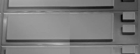
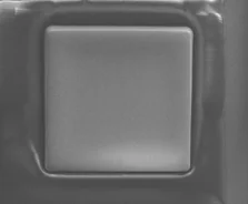
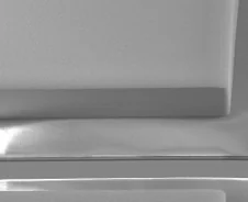
面對先進製程節點的開發成本與技術門檻持續墊高,一味追求極致微縮已非唯一解方;以異質凸塊進行複合式封裝,正成為兼顧效能與成本的主流做法。台星科可依客戶產品需求提供多種異質凸塊組合,包括「C4/CuP Bump + UBM」、「Large Bump + Small Bump」、「CuP + C4 Bump」等結構搭配。As development costs and technical barriers for advanced process nodes continue to rise, chasing further scaling is no longer the only path forward. Heterogeneous bumping — combining multiple bump structures within a single package — has become a mainstream approach to balancing performance and cost. Winstek offers a range of heterogeneous bump combinations to match customer product requirements, including C4/CuP Bump + UBM, Large Bump + Small Bump, and CuP + C4 Bump configurations.
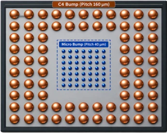
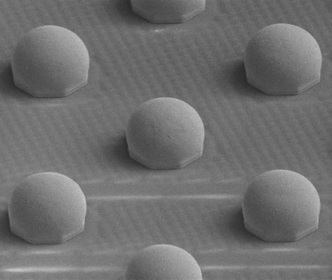
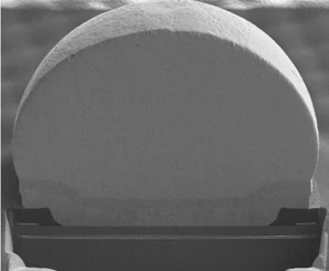
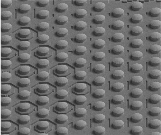
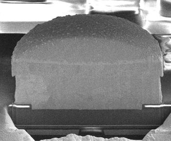
| C4 + µ-CuPC4 + µ-CuP | Large + Small BumpLarge + Small Bump | |
| Wafer Size | 300mm | 200mm |
| Die Size | 7.013 * 6.261 mm | 1.9 x 4.09mm |
| Bump Q'ty | 726 inner / 1310 outer | 3 |
| Bump Pitch | 40 inner / 160 outer (um) | 350um |
| PI CD / Thickness | 47 um / 5 um | 340um / 2940um |
| UBM Size | 20 inner / 65 outer (um) | 400um / 3000um |
| Solder Composition | SnAg 1.8% | Copper |
| Bump Structure | µ-CuP inner - Cu5 / Ni2 / LF 5 C4 outer - Cu5 / Ni3 / LF 45 | Pillar Only - Cu 100 |
玻璃晶圓圖形化製程Glass Wafer Patterning Process (TGV RDL)
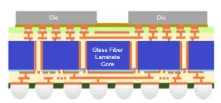
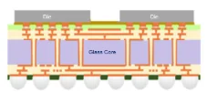
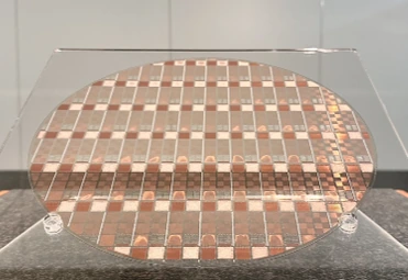
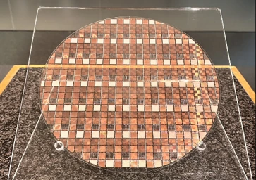
以玻璃晶圓作為基板核心,材料本身具備優異的抗翹曲能力,電氣特性也優於傳統 ABF 基板;透過玻璃穿孔(TGV)技術,可將正反雙面之 RDL 線路完美互聯,應用於先進封裝中介層,或作為極細線路載板方案。Using a glass wafer as the core substrate delivers excellent warpage resistance and superior electrical characteristics compared to conventional ABF substrates. Through-Glass-Via (TGV) technology interconnects RDL circuits on both sides — suitable as an advanced packaging interposer or as a carrier for ultra-fine line/space routing.
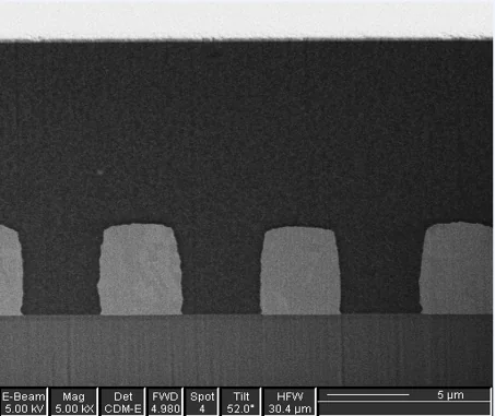
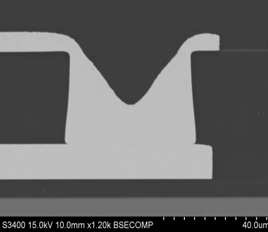
厚鈍化層堆疊製程Thick Passivation Stacking Process
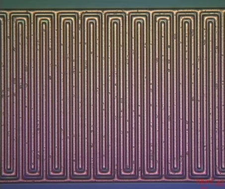
在先進封裝中,厚 PI 不僅是單純的「保護漆」,更是解決應力管理、電氣隔離與結構支撐的多功能關鍵材料,特別適用於高密度、高可靠度與柔性化的封裝需求。In advanced packaging, thick PI is far more than a simple protective coating — it is a multifunctional material for stress management, electrical isolation, and structural support, purpose-built for high-density, high-reliability, and flexible packaging needs.
| 項目Category | 液態 PI(凸塊/重佈線用途)Liquid PI (UBM / RDL) | 液態 PI(WLCSP 用途)Liquid PI (WLCSP) | 乾膜 PI(研發/試作)Dry Film PI (R&D / Prototype) |
| 厚度Thickness | 5 – 10 µm | 10 – 25 µm | 10 / 20 / 45 µm |
| 不含 NMPNMP-Free | 否No | 是Yes | 是Yes |
| 解析度(PIO/厚度)Resolution (PIO / Thickness) | 0.10 / 10 | 0.40 / 40 | 0.40 / 45 |
| 液態 PILiquid PI | 乾膜 PIDry Film PI | |
| 製程潔淨度Process Cleanliness | 較難管控Harder to control | 相較於液態 PI,其製程過程中對於粒子粉塵的管控較為容易Easier particle/dust control during processing compared to liquid PI |
| 厚度均勻性Thickness Uniformity | 較難管控Harder to control | 薄膜出貨厚度均已達到一定水準內的保證Film thickness guaranteed within a consistent range at shipment |
| 解析力Resolution | 無差異No difference | 無差異No difference |
| 固化溫度Cure Temperature | 較長的高溫固化時間Longer high-temperature cure time | 較液態 PI 為短,節省成本及減少碳排Shorter than liquid PI, reducing cost and carbon footprint |