
覆晶接合技術總覽Flip Chip Technology Overview
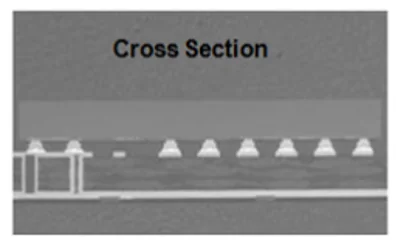
技術剖面示意Cross-Section Illustration
核心優勢Core Advantages
針對高 I/O 數晶片在運作時產生的熱能、線路電磁相容與電磁干擾(EMI)等嚴苛挑戰,台星科提供高可靠度且高效率的覆晶封裝解決方案,協助客戶在複雜電性條件下依然維持穩定的產品表現。To address the severe thermal, circuit electromagnetic compatibility, and electromagnetic interference (EMI) challenges generated during operation of high-I/O-count chips, WINSTEK provides highly reliable and efficient flip chip packaging solutions, helping customers maintain stable product performance under complex electrical conditions.
FCCSP 覆晶晶片尺寸封裝FCCSP — Flip Chip Chip Scale Package
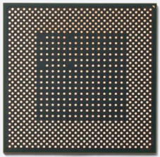
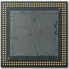
支援約 1,600 I/O 數、封裝尺寸最大達 15 x 15mm 與極細間距(Pitch ≥ 65µm)的晶片級封裝能力,適用於高整合度、輕薄化需求的先進封裝應用。Supporting approximately 1,600 I/O counts, package dimensions up to 15 x 15mm, and ultra-fine pitch (Pitch ≥ 65µm), suited for advanced packaging applications requiring high integration and thin-profile form factors.
關鍵規格Key Specifications
封裝結構種類Package Structure Types
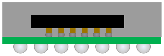
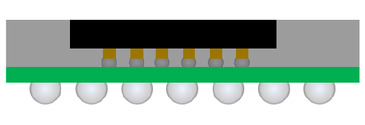
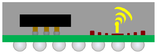
FCLGA 覆晶平面閘格陣列封裝FCLGA — Flip Chip Land Grid Array
以平面焊墊(Land)取代錫球作為對外接點,封裝整體高度更低,適合追求輕薄化的覆晶封裝應用。Uses flat lands instead of solder balls as external contacts, lowering the overall package height for flip chip applications that require a thin profile.
封裝結構種類Package Structure Types


FCBGA 覆晶球柵陣列封裝FCBGA — Flip Chip Ball Grid Array
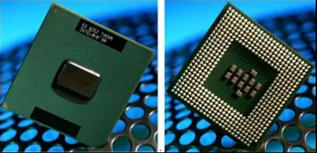
具備支援高達約 27,000 I/O 數、極致封裝尺寸(最大達 55 x 55mm)與極細間距(Pitch ≥ 65µm)的封裝量產能力,因應高複雜度晶片的先進封裝需求。High-volume production capability supporting up to approximately 27,000 I/O counts, extreme package dimensions (up to 55 x 55mm), and ultra-fine pitch (Pitch ≥ 65µm), meeting the advanced packaging needs of highly complex chips.
關鍵規格Key Specifications
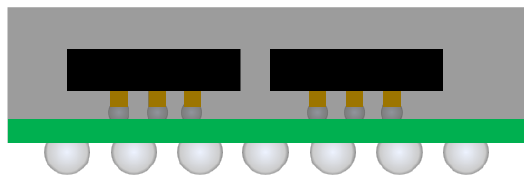
MCM 多晶片模組封裝MCM — Multi-Chip Module
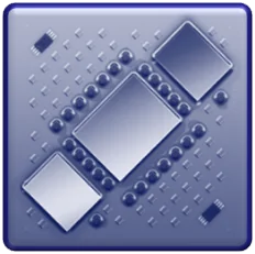
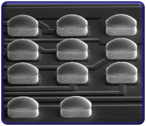
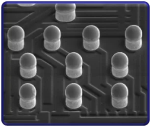
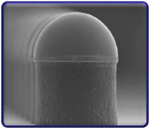
展現高度集成的系統級封裝實力,可於單一載板上進行多種不同功能的晶片互連,實現低訊號損耗、高效能的系統級晶片(SoC),目前已可穩定支援最多三晶片於一載板之設計。Demonstrating highly integrated system-in-package capability, enabling interconnection of multiple functionally distinct chips on a single substrate to achieve low-signal-loss, high-performance system-on-chip (SoC) designs — currently supporting stable designs of up to three chips on a single substrate.
關鍵能力Key Capability
規格比較總表(WLCSP/FCCSP/FCBGA)Specification Comparison (WLCSP / FCCSP / FCBGA)
| 規格項目Specification Item | WLCSP | FCCSP | FCBGA |
|---|---|---|---|
| I/O Count | < 250 | 約 1,600~1,600 | 約 27,000~27,000 |
| Die Size | ≤ 6 x 6mm | ≤ 12 x 12mm | ≤ 30 x 30mm |
| Package Size | — | ≤ 15 x 15mm | ≤ 55 x 55mm |
| Bump Pitch | 350-500µm | ≥ 65µm | ≥ 65µm |
| Bump Height | 200-300µm | ≥ 50µm | ≥ 50µm |
| Solder Ball Pitch | — | ≥ 200µm | ≥ 350µm |
| Solder Ball Size | — | ≥ 130µm | ≥ 150µm |
| Under-fill | — | Mold (MUF) | UF |
應用領域Applications
廣泛支援多元晶片應用,橫跨邏輯、電源管理、射頻、感測與記憶體等領域:Broad support across logic, power management, RF, sensing and memory applications:
AP・UC Controller
PMU
RF・PA
MEMS & Sensor
EEPROM・DRAM・Flash・SRAM
Smart Card