繁中 | EN 聯絡我們Contact Us
DPS

晶粒處理服務Die Processing Services

從晶圓薄化到裸晶切割封裝,以先進製程工藝與嚴謹品質管控,確保晶片良率與供應穩定性。With advanced wafer grinding and die-level dicing and packaging processes under rigorous quality control, we ensure high yield and reliable supply for our customers.

DIE PROCESSING SERVICES (DPS)

裸晶切割封裝服務Die Processing Services

台星科提供從晶圓薄化(Wafer Grinding)、精密切割(Saw)、到包裝出貨(Tape & Reel)的完整一站式服務(One-Stop Shop),透過高度整合的前段製程,協助封裝測試客戶簡化繁複供應鏈、提升量產穩定度,並確保後段封裝與測試階段的最高良率。WINSTEK offers a fully integrated one-stop service spanning wafer grinding, precision sawing, and packaging/shipment (tape & reel). Through highly integrated front-end processes, we help OSAT and test customers simplify complex supply chains, improve mass-production stability, and ensure maximum yield in downstream packaging and test operations.

核心技術與優勢Core Technologies & Advantages

極致薄化與高應力晶圓處理(Wafer Grinding)Ultra-Thin Grinding & High-Stress Wafer Handling (Wafer Grinding)

支援 250µm 以下超薄晶圓 In-Line Grinding、100µm 以下 DBG(Dicing Before Grind)先進工藝,並具備處理高應力(High Stress)與高地貌(High Topography)晶圓的工藝能力。Supports in-line grinding for ultra-thin wafers below 250µm and advanced DBG (Dicing Before Grinding) below 100µm, with process capability for handling high-stress and high-topography wafers.

可追溯晶粒的晶背雷射印碼(Laser Marking)Traceable Die Laser Marking on Wafer Back (Laser Marking)

以 Stand-alone Marking 或 Marking through tape 兩種工藝,針對 Si、BSL、Ag、Cu、Ni 晶背材質皆可藉由雷射印碼,以字碼或二維條碼提供批號、刻號、座標軸以供日後品質追溯。Using either stand-alone marking or marking through tape, laser marking can be applied to Si, BSL, Ag, Cu and Ni wafer backsides, recording lot number, wafer ID and die coordinates as alphanumeric text or 2D codes for future quality traceability.

高精密微間距切割(Wafer Saw & Singulation)High-Precision Fine-Pitch Dicing (Wafer Saw & Singulation)

靈活運用雷射溝槽(Laser Groove)與傳統刀片切割(Conventional Blade Saw),對應 Si Low-k、NOR Flash、GaN、SiC、Glass 等先進半導體材料,以及 BSM(Ag、Cu、Ni) 與堆疊晶圓(Stacking Wafer)。Flexibly combines Laser Groove and conventional blade sawing to address advanced materials such as Si Low-k, NOR Flash, GaN, SiC, and Glass, as well as BSM (Ag, Cu, Ni) and stacked wafers.

嚴格品管與智慧出貨交付(Tape & Reel)Rigorous Quality Control & Smart Shipment Delivery (Tape & Reel)

支援 Tape & Reel、Wafer on Ring 與 Reel-to-Reel 轉換,具備 5 面光學檢驗(正面、背面、側壁)、IR 檢測/Flipper 和Non-Flipper 技術及完整的 Die Traceability(晶粒履歷追蹤)。Supports Tape & Reel, Wafer on Ring, and reel-to-reel conversion, with 5-side optical inspection (top, bottom, sidewalls), IR inspection/flipper and non-flipper technology, and full die traceability.

規格能力表Specifications & Capability Table

製程項目Process 技術規格Technical Specification
Grinding 晶圓厚度:< 100µm|支援 High Stress/High Topography WaferWafer thickness: < 100µm | Supports High Stress / High Topography wafers
Laser Marking 晶背材質:Si、BSL、Ag、Cu、Ni|晶圓形式:Wafer form、Ring frame formWafer back materials: Si, BSL, Ag, Cu, Ni | Wafer form: Wafer form, Ring frame form
Singulation 材料:Si Low-k/NOR Flash/GaN/SiC / Glass|晶圓形式:CSP/BSM/Stacking WaferMaterials: Si Low-k / NOR Flash / GaN / SiC / Glass | Wafer types: CSP / BSM / Stacking Wafer
Tape & Reel Die Size:0.3 × 0.3 mm ~ 12.0 × 9.0 mm|Thickness:50 ~ 1500 µmDie size: 0.3 × 0.3 mm – 12.0 × 9.0 mm | Thickness: 50 – 1500 µm
Tape & Reel 支援條件Tape & Reel Support Conditions
項目Item 規格Specification
供料方式Feeding Type Wafer on Ring
晶圓厚度Wafer Thickness 50~1500µm
包裝形式Package Reel

為客戶創造的關鍵價值Key Value Delivered to Customers

DPS 可與前段 Bump 與後段 CP + Assy 進行整合,提供 Turnkey 服務,降低客戶的管理成本。DPS can be integrated with front-end bumping and back-end CP and assembly to provide a turnkey service, lowering customers’ management costs.
支援超薄、高應力及高硬度新世代材料,化解物理瓶頸。Supports ultra-thin, high-stress, and high-hardness advanced materials, overcoming physical process bottlenecks.
可直接銜接封裝線,降低二次處理風險。Connects directly to packaging lines, reducing secondary-handling risk.
完整 Traceability,符合高可靠度應用。Full traceability meets the demands of high-reliability applications.

適用客戶Target Customers

OSAT/IDM 封裝單位OSAT / IDM Packaging Units 功率/車用/工業晶片製造商Power / Automotive / Industrial Chip Manufacturers Fabless IC 設計公司Fabless IC Design Companies

關鍵亮點Key Highlights

One-Stop Die Processing Services 100µm 以下超薄晶圓能力Sub-100µm Ultra-Thin Wafer Capability Si/GaN/SiC/Low-k/BSM/Stacking全覆蓋Full Coverage Tape & Reel 即用型交付Ready-to-Use Delivery
WAFER GRINDING

晶圓薄化製程Wafer Grinding Process

在追求輕薄短小的先進封裝趨勢下,晶圓薄化面臨著極高的應力與翹曲(Warpage)挑戰。我們透過嚴謹的關鍵製程參數管控與高階設備,從研磨保護膠帶的精準貼合、乾式拋光研磨的表面品質,到 In-Line 系統整合與製程解決方案,全面守護超薄晶圓在製程中的穩定度與平坦度,滿足客戶對高品質極限厚度的嚴苛期待。Amid the drive toward thinner, lighter advanced packaging, wafer thinning faces significant stress and warpage challenges. Through rigorous control of critical process parameters and advanced equipment—from precision lamination of grinding protective tape and dry-polish surface quality, to In-Line system integration and tailored process solutions—we safeguard the stability and flatness of ultra-thin wafers throughout processing, meeting customers’ most demanding requirements for extreme thickness reduction.

核心製程優勢Core Process Advantages

研磨保護膠帶Grinding Protective Tape
精準貼合的研磨保護膠帶,全面保護晶圓表面免受研磨過程損傷。Precisely applied grinding protective tape fully shields the wafer surface from damage during grinding.
乾式拋光研磨Dry Polish Grinding
提供優異的表面平坦度與品質,取代傳統濕式製程可能帶來的化學殘留風險。Delivers superior surface flatness and quality, eliminating the chemical-residue risks associated with conventional wet processes.
In-Line 系統整合In-Line System Integration
有效克服超薄晶圓在製程間傳遞時的翹曲挑戰,確保穩定支撐與精準定位。Effectively overcomes warpage challenges during inter-process transport of ultra-thin wafers, ensuring stable support and precise positioning.
製程解決方案Process Solutions
DBG、SDBG、TBDB、異徑研磨,完善工程經驗,滿足客戶新產品開發需求。DBG, SDBG, TBDB and variable-diameter grinding, backed by comprehensive engineering experience to support customers’ new product development.

規格與能力表Specifications & Capability Table

Wafer THK 50µm 75µm 100µm 150µm 250µm 750µm
DAG 無凸塊晶圓No bump wafer
凸塊高度 ≤ 170µm 晶圓≤ 170µm bump height wafer
DBG 無凸塊晶圓No bump wafer
凸塊高度 ≤ 170µm 晶圓≤ 170µm bump height wafer
SDBG 無凸塊晶圓 & 凸塊高度 ≤ 170µm 晶圓No bump wafer & ≤ 170µm bump height wafer
SDTT 無凸塊晶圓 & 凸塊高度 ≤ 170µm 晶圓No bump wafer & ≤ 170µm bump height wafer
BACKSIDE LASER MARKING

晶背雷射印碼Backside Laser Marking

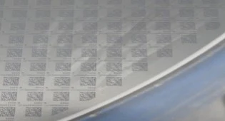
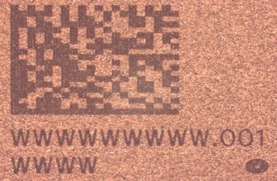
晶圓晶背雷射印碼(Wafer Backside Laser Marking)在不破壞正面電路的前提下,為晶粒提供永久的「身分證」,以實現全製程的追溯與良率管理。支援裸片晶圓(Stand-alone)以及帶鐵圈的薄晶圓(Marking through tape),對應 Si、BSL、Ag、Cu、Ni 晶背材質的雷射印碼,以及 2D Code 的雷射印碼。Wafer backside laser marking gives each die a permanent identity without damaging front-side circuitry, enabling full-process traceability and yield management. It supports stand-alone wafers as well as thin wafers on frames (marking through tape), covering Si, BSL, Ag, Cu and Ni backside materials, together with 2D code laser marking.


對應各種晶背材質雷射印碼Laser Marking for Various Backside Materials
Laser marking sample on wafer backside Laser marking sample on wafer backside Laser marking sample on wafer backside
2D Matrix Marking2D Matrix Marking
2D matrix code laser marking on wafer
SAWING / DICING

切割服務Dicing Services

面對新世代介電層材料(如 Low-K 等易脆特性),傳統單純刀輪切割極易產生微小暗裂(Micro-cracks)並導致晶片功能失效。我們透過導入先進的雷射開槽技術(Laser Groove)與多元切割解決方案,完美克服材料極限,確保每一個晶粒的邊緣結構完整。無論是標準晶圓、極窄切割道需求,或是碳化矽(SiC)、Glass、GaN、BSM、Stacking Wafer等特殊晶圓,我們皆能提供全方位的專業代工與製程整合能力。Advanced dielectric materials (such as brittle low-k films) are prone to micro-cracking and functional failure under conventional blade dicing alone. By adopting advanced Laser Groove technology alongside diverse dicing solutions, we overcome these material limitations and preserve the structural integrity of every die edge. Whether standard wafers, ultra-narrow scribe-line requirements, or specialty wafers such as SiC, Glass, GaN, BSM, and stacked wafers, we deliver comprehensive foundry service and process integration capability.

核心切割技術Core Dicing Technologies
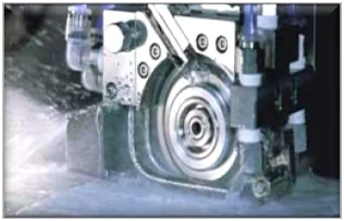
Blade SAW
Blade SAW
傳統與精密刀輪切割,適用絕大多數標準晶圓的量產切割需求。Conventional and precision blade sawing for the mass-production dicing needs of most standard wafers.
Laser Groove
Laser Groove
雷射開槽技術,有效降低切割應力與微裂紋風險,因應 Low-K 等易脆材料。Laser grooving technology effectively reduces dicing stress and micro-crack risk for brittle materials such as low-k films.
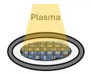
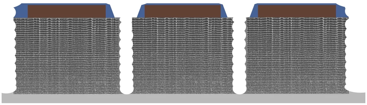
Plasma Dicing (Co-develop with customer)
Plasma Dicing Plasma dicing die sidewall cross-section
電漿切割技術,實現無應力、高精度的晶粒分離。Plasma dicing technology achieves stress-free, high-precision die separation.
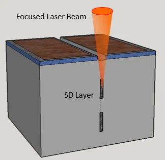
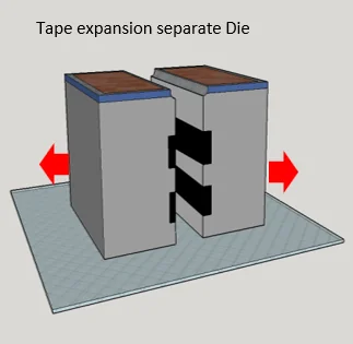
Stealth Dicing & 擴片Wafer Expansion
Focused Laser Beam Tape expansion separate Die
隱形切割與晶粒分離製程,並支援碳化矽(SiC)等特殊晶圓於廠內對應施作。Stealth dicing and die separation processes, with in-house capability for specialty wafers such as SiC.

規格與能力表Specifications & Capability Table

製程就緒Process ready 製程建置中Process installation in progress 需評估Need evaluation
晶圓厚度(µm)Wafer Thickness (µm) 切割道寬度 Saw Street Width(µm)Saw Street Width (µm)
303540455055606570758085≥90
50
75
100
150
200
300
400
500
600
700
750
不研磨No grinding
TAPE & REEL SERVICE

捲帶包裝與出貨Tape & Reel Service

載帶寬度與晶粒尺寸對應Carrier Tape Width vs. Die Size Range

載帶寬度Carrier Tape Width 晶粒尺寸範圍(mm)Die Size Range (mm)
8mm 0.2 × 0.4 ~ 3.0 × 3.0
12mm > 3.0 × 3.0 ~ 6.0 × 6.0
16mm > 6.0 × 6.0 ~ 10.0 × 10.0
24mm > 10.0 × 10.0 ~ 15.0 × 15.0

捲帶包裝流程Tape & Reel Process Flow

  1. 01Wafer / Die Input晶圓/晶粒投入
  2. 02Die Picking & Orientation晶粒取放與方向校正
  3. 03Multi Vision Inspection多視角光學檢測
  4. 04Tape & Reel Packaging捲帶包裝
  5. 052D Code Reading & Traceability二維條碼讀取與追溯
  6. 06Finished Reel完成捲盤