環境應力試驗Environmental Stress Testing
濕度敏感等級區分(Moisture Sensitivity Level, MSL)Moisture Sensitivity Level (MSL)
針對表面黏著型元件(SMD)或需經過 SMT 迴焊(Reflow)之零件進行驗證。主要以超音波掃描(SAT/SAM)判斷脫層(Delamination)位置與脫層比率,藉以制定濕度敏感等級。Validates surface-mount devices (SMD) requiring SMT reflow. Delamination location and ratio are determined via ultrasonic scanning (SAT/SAM) to classify moisture sensitivity level.
測試條件:等級分布為 Level 1 至 Level 6,主要差異在於零件吸濕條件。Test conditions: Levels range from Level 1 to Level 6, differentiated primarily by component moisture-absorption conditions.
| LEVEL | FLOOR LIFE | SOAK REQUIREMENTS | |||||
|---|---|---|---|---|---|---|---|
| STANDARD | ACCELERATED EQUIVALENT | ||||||
| eV 0.40-0.48 |
eV 0.30-0.39 |
CONDITION | |||||
| TIME | CONDITION | TIME (hours) | condition | TIME (hours) | TIME (hours) | ||
| 1 | Unlimited | ≤ 30°C/85%RH | 168+5/-0 | 85°C/85%RH | NA | NA | NA |
| 2 | 1 year | ≤ 30°C/60%RH | 168+5/-0 | 85°C/60%RH | NA | NA | NA |
| 2a | 4 weeks | ≤ 30°C/60%RH | 696+5/-0 | 30°C/60%RH | 120+1/-0 | 168+1/-0 | 60°C/60%RH |
| 3 | 168 hours | ≤ 30°C/60%RH | 192+5/-0 | 30°C/60%RH | 40+1/-0 | 52+1/-0 | 60°C/60%RH |
| 4 | 72 hours | ≤ 30°C/60%RH | 96+2/-0 | 30°C/60%RH | 20+0.5/-0 | 24+0.5/-0 | 60°C/60%RH |
| 5 | 48 hours | ≤ 30°C/60%RH | 72+2/-0 | 30°C/60%RH | 15+0.5/-0 | 20+0.5/-0 | 60°C/60%RH |
| 5a | 24 hours | ≤ 30°C/60%RH | 48+2/-0 | 30°C/60%RH | 10+0.5/-0 | 13+0.5/-0 | 60°C/60%RH |
| 6 | Time on Label (TOL) | ≤ 30°C/60%RH | TOL | 30°C/60%RH | NA | NA | NA |
參考規範:IPC/JEDEC J-STD-020, JESD22-A113Reference standards: IPC/JEDEC J-STD-020, JESD22-A113
溫度循環試驗(Temperature Cycling Test, TC)Temperature Cycling Test (TC)
可靠度試驗中相當重要的一項。藉由冷熱交替變換多個循環,因膨脹係數差異造成對產品的疲勞老化(Fatigue)影響。A key reliability test. Repeated hot/cold cycling induces fatigue effects due to differing thermal expansion coefficients.
測試條件:以每分鐘 5~15 度的溫變率進行連串的高、低溫週期測試。施加應力於待測物上加速老化因素,使樣品產生潛在損害,以決定試件是否正確設計或製造。Test condition: successive high/low temperature cycles at a rate of 5–15°C/min, accelerating aging factors to reveal design or manufacturing defects.
溫度衝擊試驗(Thermal Shock Test, TS)Thermal Shock Test (TS)
評估產品生命週期中面臨極端環境條件時脆弱部位的損傷或失效,進而確保產品可靠度。Assesses damage or failure at vulnerable points under extreme environmental conditions, ensuring product reliability.
測試條件:以每分鐘 40 度以上的急劇溫變率做極嚴苛條件之高、低溫衝擊測試,加速老化因素並展現高品質測試環境與設備驗證實力。Test condition: extreme high/low temperature shock at a rate above 40°C/min, accelerating aging factors under rigorous validation conditions.
參考規範:JESD 22-A104, JESD 22-A106Reference standards: JESD 22-A104, JESD 22-A106
高加速溫濕度試驗(Highly Accelerated Stress Test, HAST)Highly Accelerated Stress Test (HAST)
提高環境應力(如溫度)與工作應力(電壓、負荷),加速試驗過程,縮短產品或系統的壽命試驗時間,調查分析電子元件與機械零件的摩耗與使用壽命問題。Elevates environmental stress (temperature) and operating stress (voltage, load) to accelerate the test, shortening life-test duration and investigating wear and lifespan issues.
| Temperature [dry bulb °C] |
Relative Humidity[%] |
Temperature [wet bulb, °C] |
Vapor Pressure [kPa (psia)] |
Duration [hours] |
|---|---|---|---|---|
| 130 ± 2 | 85 ± 5 | 124.7 | 230 (33.3) | 96 +2/-0 |
| 110 ± 2 | 85 ± 5 | 105.2 | 122 (17.7) | 264 +2/-0 |
高溫水蒸氣壓力試驗(Pressure Cooker Test, PCT/Autoclave)Pressure Cooker Test (PCT/Autoclave)
一般稱為壓力鍋蒸煮試驗或飽和蒸氣試驗,將待測品置於嚴苛之溫度、飽和濕度(100% R.H. 飽和水蒸氣)及壓力環境下測試,測試待測品耐高濕能力。Also known as autoclave testing, subjecting samples to severe temperature, saturated humidity (100% R.H.) and pressure to assess high-humidity resistance.
| Temperature [dry bulb °C] | Relative Humidity [%] | Vapor Pressure [psia/kPa] |
|---|---|---|
| 121 ± 2 | 100% | 29.7 / 205 |
HAST/PCT 參考規範:JESD 22-A110, JESD 22-A118, JESD 22-A102HAST/PCT reference standards: JESD 22-A110, JESD 22-A118, JESD 22-A102
IC 老化試驗IC Burn-In & Life Testing
IC 老化試驗核心技術原理Core Technology & Testing Methods
以加速溫度、電壓等環境與工作應力,在短時間內精準預估 IC 的使用壽命與生命周期。試驗過程中均需加入電源與信號源,使 IC 進入工作狀態或穩態,經由電壓、溫度、時間等加速因子(Acceleration Factor)的交互作用,達成材料老化效應。Accelerated temperature and voltage stress precisely estimates IC lifespan within a short time. Power and signal sources drive the IC into an operating or steady state, and the interaction of voltage, temperature, and time acceleration factors produces material aging effects.
針對不同產品特性提供專屬測試方法,完全滿足 HTGB(High Temperature Gate Bias)、HTRB(High Temperature Reverse Bias)、BLT(Bias Life Test)等嚴格試驗要求。Dedicated test methods for different product types, fully meeting rigorous HTGB, HTRB, and BLT test requirements.
測試條件與試驗類型Testing Conditions & Applications
利用高溫及電壓加速應力,評估 IC 長時間的使用壽命。試驗中運用動態訊號,以符合實際的產品使用狀態。Uses high-temperature and voltage stress to assess long-term IC lifespan, with dynamic signals matching real-world usage.
利用高溫及電壓加速應力,精準篩選出早夭產品,以利評估與掌控產品的早夭率。High-temperature and voltage stress precisely screens out early-failure units, enabling accurate assessment and control of early failure rate.
國際標準與參考規範Standards & Specifications
參考規範:JESD 22-A108Reference standard: JESD 22-A108
靜電防護 / 閂鎖試驗ESD & Latch-Up Testing
ESD 實驗室核心能量與一站式驗證ESD Lab Capability & Full-Service Solutions
靜電防護是 IC 半導體產品需應用的內建式電路防護要求,須抵抗外界所有電性對於內建積體電路的破壞。ESD protection is a built-in circuit requirement for IC semiconductor products, defending against all external electrical damage to the embedded circuitry.
Winstek ESD 實驗室除了可提供 MIL、JDEC、ANSI、IEC、AECQ 等 ESD 測試規範之外,同時提供靜電防護測試服務,以及測試之後的 Final test 及 FA(失效分析)等完整驗證分析服務,並具備專屬 ESD 試驗 Socket 與轉板的設計製作能力。The Winstek ESD lab supports MIL, JEDEC, ANSI, IEC, and AEC-Q test specifications, plus ESD testing, downstream Final Test, and FA (failure analysis), with in-house design and fabrication of dedicated ESD test sockets and adapter boards.
測試條件與項目Testing Modes & Measurement
國際相容標準與參考規範Standards & Compliance
板階可靠度驗證Board Level Reliability (BLR)
機械衝擊試驗(Mechanical Shock Test)Mechanical Shock Test
評估 IC 封裝打件後,在製程、包裝、運輸及正常使用時,由於電路板受動態劇烈變形時,焊點接合位置(Solder Joint)是否產生新型破壞而影響使用壽命。Assesses whether solder joints suffer new failure modes affecting lifespan when the PCB undergoes dynamic deformation during processing, packaging, transport, or normal use.
| Service Condition | Equivalent Drop Height (in/cm) | Velocity Change (in/s/cm/s) | Acceleration Peak (G) | Pulse Duration (ms) |
|---|---|---|---|---|
| H | 59 / 150 | 214 / 543 | 2900 | 0.3 |
| G | 51 / 130 | 199 / 505 | 2000 | 0.4 |
| B | 44 / 112 | 184 / 467 | 1500 | 0.5 |
| F | 30 / 76.2 | 152 / 386 | 900 | 0.7 |
| A | 20 / 50.8 | 124 / 316 | 500 | 1 |
| E | 13 / 33.0 | 100 / 254 | 340 | 1.2 |
| D | 7 / 17.8 | 73.6 / 187 | 200 | 1.5 |
| C | 3 / 7.62 | 48.1 / 122 | 100 | 2 |
參考規範:JESD 22-B104, JESD 22-B111Reference standards: JESD 22-B104, JESD 22-B111
震動試驗(Vibration Test)Vibration Test
產品受到震動應力效應時,震動達到重複應力引起疲勞,容易造成板階(Board Level)焊點斷裂;同時零組件因組裝方式或機構設計的自然頻率響應,受到震動激發產生共振響應(Resonance Amplification)現象對結構損害較大。Repeated vibration stress induces fatigue that can crack board-level solder joints; components' natural frequency response can also trigger resonance amplification, causing greater structural damage.
| Service Condition | Peak Acceleration (G) | Displacement pk-pk (in/mm) | Cross-over Frequency (Hz) | Min./Max. Frequency (Hz) |
|---|---|---|---|---|
| 1 | 20 | 0.060 / 1.5 | 80 | 20 / 2000 |
| 2 | 10 | 0.040 / 1.0 | 70 | 10 / 1000 |
| 3 | 3 | 0.030 / 0.75 | 45 | 5 / 500 |
| 4 | 1 | 0.020 / 0.5 | 31 | 5 / 500 |
| 5 | 0.3 | 0.010 / 0.25 | 24 | 5 / 500 |
| 6 | 0.1 | 0.005 / 0.125 | 20 | 5 / 500 |
| 7 | 0.01 | 0.001 / 0.039 | 14 | 5 / 500 |
| 8 | 0.01 | 0.0005 / 0.0127 | 6.2 | 5 / 500 |
參考規範:JESD 22-B103, MIL-STD 883 method 2007, ASTM D4169Reference standards: JESD 22-B103, MIL-STD 883 method 2007, ASTM D4169
板階溫度循環試驗(Board Level Temperature Cycling Test)Board Level Temperature Cycling Test
評估表面黏著零件時,在溫度冷熱循環的疲勞效應下,焊點材料潛性的機械疲勞與變形的情形,可了解產生的潛在危害系統及零組件的因素。Assesses latent mechanical fatigue and deformation of solder joint materials in SMD components under thermal cycling, revealing potential system and component risk factors.
| Test Condition | Nominal Ts(min) (°C) with Tolerances | Nominal Ts(max) (°C) with Tolerances |
|---|---|---|
| A | -55(+0, -10) | +85(+10, -0) |
| B | -55(+0, -10) | +125(+15, -0) |
| C | -65(+0, -10) | +150(+15, -0) |
| G | -40(+0, -10) | +125(+15, -0) |
| H | -55(+0, -10) | +150(+15, -0) |
| I | -40(+0, -10) | +115(+15, -0) |
| J | -0(+0, -10) | +100(+15, -0) |
| K | -0(+0, -10) | +125(+15, -0) |
| L | -55(+0, -10) | +110(+15, -0) |
| M | -40(+0, -10) | +150(+15, -0) |
| N | -40(+0, -10) | +85(+10, -0) |
參考規範:JESD 22-A104, IPC-9701Reference standards: JESD 22-A104, IPC-9701
SMT 樣品製備生產服務SMT Sample Preparation & Assembly Services
表面元件黏著技術服務核心優勢SMT Core Technical Strengths
SMT 製程是板階可靠度試驗的首要關鍵站點,IC 黏著在 PCB 上的品質直接影響產品試驗結果判斷的正確性。品質關鍵因素包括錫膏、印刷參數設定(如脫模間距及時間、印刷速率)、置件精度與鋼板設計。SMT is the first critical checkpoint for board-level reliability. IC-to-PCB attachment quality directly affects test result accuracy, with key factors including solder paste, print parameters (separation distance/time, print speed), placement accuracy, and stencil design.
Winstek 已建置一條完整 SMT 量產線,協助客戶進行組裝服務:Winstek operates a complete SMT production line to support customer assembly services:
SPI 設備可進行 Cpk 計算,嚴格掌控錫膏印刷品質。SPI equipment performs Cpk calculations for strict solder paste print quality control.
可提供氮氣與含氧量管制,使焊點品質最佳化。Nitrogen and oxygen level control optimizes solder joint quality.
針對 WLCSP 產品提供客戶 Underfill(底充膠)製程服務。Underfill process services tailored for WLCSP products.
因應零件小型化需求,提供精度達 0.20mm Pitch 的 Mounter(貼片機),滿足各類晶片尺寸與 Fine Pitch 之高階製程需求。Mounters with precision down to 0.20mm pitch, meeting fine-pitch and miniaturized component requirements.
SMT 完整製造流程SMT Manufacture Flow
高階 SMT 設備陣容Advanced SMT Equipment Platforms
配置 Panasonic 高精度 Solder Paste Printer(錫膏印刷機)與 Chip Mounter(高階貼片機)。Panasonic high-precision Solder Paste Printer and advanced Chip Mounter.
配置 ersa 高階 Reflow Oven(工業級迴焊爐系統),提供極致的熱傳導與穩定溫控實力。ersa industrial-grade Reflow Oven delivering superior heat transfer and stable temperature control.
電性分析Electrical Failure Analysis (EFA)
8" 點針台(8" Manual Prober Station)8" Manual Prober Station
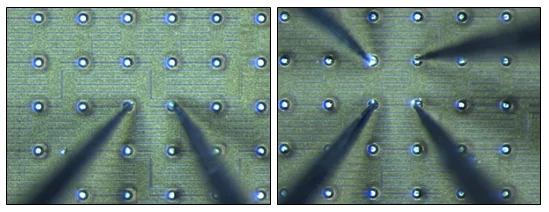
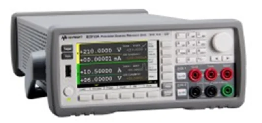
電性量測是為了驗證及量測半導體電子元件的參數與特性。利用點針(≤ 4 Probers),搭接於 IC 電路,使其可以外接各電性量測儀器,以量測電性特性。Electrical measurement validates and measures semiconductor device parameters. Manual probes (≤4 probers) contact the IC circuit, connecting external instruments to measure electrical characteristics.
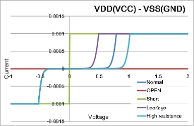
I-V 特性量測(I-V Curve Trace & Parameter Measurement)I-V Curve Trace & Parameter Measurement
量測元件之電性參數及特性。量測原理是利用自動曲線追蹤儀電特性量測的方式,快速計算阻值,藉此確認各電路關係並即時篩檢出異常(Open/Short/Leak/High Resistance)。Measures device electrical parameters using an automated curve tracer, rapidly calculating resistance to confirm circuit relationships and screen anomalies (Open/Short/Leak/High Resistance).
紅外線顯微鏡(Infrared Microscope, IR Microscope)Infrared Microscope (IR Microscope)
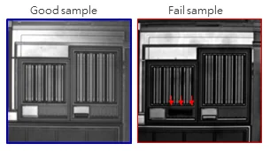
主要原理是利用紅外光波長穿透矽基材,來直接觀察元件主動區影像,精準比對好壞品差異。Infrared wavelengths penetrate the silicon substrate to directly image the active device region, precisely comparing good vs. failed units.
原子力顯微鏡(Atomic Force Microscope, AFM)Atomic Force Microscope (AFM)
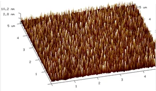
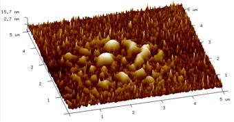
工作機制是藉由針尖與試片間的原子作用力,使懸臂樁產生微細位移,以測得樣品表面形貌。Atomic forces between the tip and sample cause minute cantilever deflection, mapping the sample's surface topography.
非破壞分析Non-Destructive Analysis (NDA)
超音波掃描(Scanning Acoustic Tomography, SAT)Scanning Acoustic Tomography (SAT)
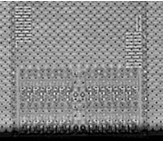
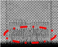
超音波顯微鏡(SAT)可穿透一定厚度的固態與液態物質,並檢測其結構組成是否有異常。藉由超音波於不同材料之反射速率及能量不同的特性進行分析。利用純水當介質傳遞超音波訊號,當訊號遇到不同材料的介面時,會部分反射、部分穿透,機台接收這些訊號組合成影像。SAT penetrates solid and liquid materials of certain thickness to detect structural anomalies, analyzing differences in reflection rate and energy across materials. Ultrasonic signals travel through a water medium; at material interfaces, signals partially reflect and partially transmit, and the received signals are composed into an image.
2D/3D X 射線檢測(2D/3D X-Ray Inspection & 3D X-Ray Microscope)2D/3D X-Ray Inspection & 3D X-Ray Microscope
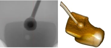
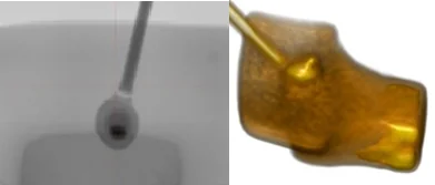
X-ray 成像方式運用 X-ray 對物品的穿透力來進行物品內部結構中密度差異的地方穿透成像。3D X-Ray 顯微鏡(3D X-Ray Microscope)是以非破壞性 X 射線透視的技術,再搭配光學物鏡提高放大倍率進行實驗檢測。實驗過程將待測物固定後進行旋轉,過程中收集各個不同角度的 2D 穿透影像,之後利用電腦運算重構成待測物體之實體影像。X-ray imaging exploits penetration power to reveal internal density variations. The 3D X-Ray Microscope combines non-destructive X-ray transmission with optical magnification; the sample rotates while 2D transmission images are captured at multiple angles and computationally reconstructed into a 3D image.
3D 雷射顯微鏡(3D Laser Optical Microscope, 3D Laser OM)3D Laser Optical Microscope (3D Laser OM)
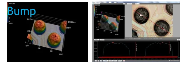
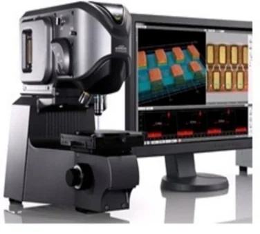
3D Laser OM 原理是藉由一般可見光對物體表面之反射特性,透過光學的透鏡放大、縮小及 CCD 來擷取影像,可進行表面形貌的觀察與尺寸的分析量測,並利用雷射光源來量測出精準的 Z 軸輪廓。3D Laser OM captures images via visible-light surface reflection through optical magnification and a CCD sensor, enabling surface topography observation and dimensional analysis, with a laser source measuring precise Z-axis profiles.
破壞性分析Destructive Physical Analysis (DPA)
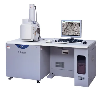
掃描式電子顯微鏡(Scanning Electron Microscope, SEM)Scanning Electron Microscope (SEM)
掃描電子顯微鏡(SEM)是表面微細結構觀察最快速有效的方法,利用微小聚焦的電子束(Electron Beam)進行樣品表面掃描,以收集二次電子訊號來成像。訊號源主要來自二次電子、背向散射電子及特性 X 光等。SEM 可提供樣品表面高解析度且長景深的圖像,極利於微小區域的觀察。同時結合 EDS(X-射線能量散佈布能譜)進行元素成分分析。SEM is the fastest, most effective method for observing fine surface structures, using a focused electron beam to scan the sample and collect secondary-electron signals for imaging. Signals derive mainly from secondary electrons, backscattered electrons, and characteristic X-rays. SEM provides high-resolution, deep-focus images ideal for micro-region observation, combined with EDS for elemental composition analysis.
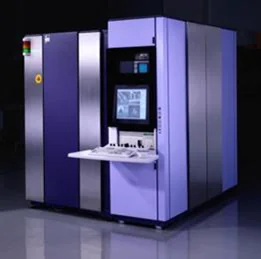
12” 晶圓級雙束聚焦離子束(12" Wafer-Level Dual Beam FIB)12" Wafer-Level Dual Beam FIB
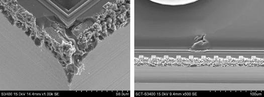
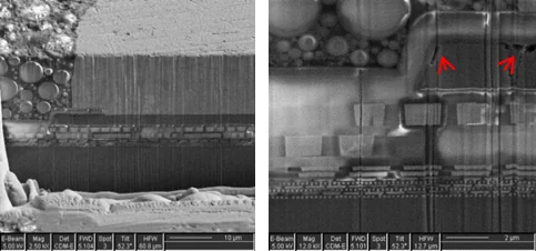
12 吋晶圓級雙束聚焦離子束(Dual Beam FIB)機台能在使用離子束切割樣品的同時,用電子束對樣品斷面進行即時觀察,亦能進行 EDX 的成分分析。The 12" wafer-level Dual Beam FIB system cuts samples with an ion beam while simultaneously observing the cross-section in real time with an electron beam, also supporting EDX composition analysis.
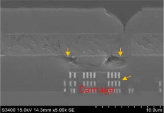
切片破壞分析(Cross-Section Analysis/Polishing)Cross-Section Analysis/Polishing
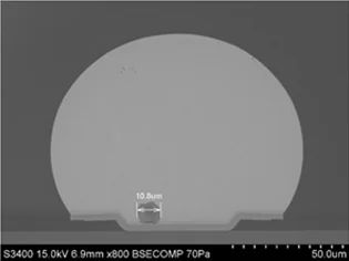
用混合膠填滿樣品周圍縫隙,以增強樣品結構強度,避免因承受研磨應力而樣品毀損。樣品以不同粗細之砂紙,在特定區域(定點)或非特定區域(非定點)進行研磨後觀察。Compound resin fills the surrounding gaps to reinforce sample structural integrity, preventing damage from polishing stress. Samples are polished with sandpaper of varying grits, either at a targeted or non-targeted location, before observation.
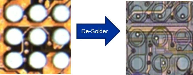
化性破壞分析(Chemical Decapsulation & De-solder Analysis)Chemical Decapsulation & De-solder Analysis
利用蝕刻液進行濕式蝕刻,執行開蓋(Decap)、去膠(去除封膠,Compound Removal)、取出晶粒、去錫球等步驟,觀察封膠體內晶片或元件異常問題(如:打線異常、晶片 Crack、chipping、刷痕....等)。Wet etching performs decapsulation, compound removal, die extraction, and de-soldering, revealing die/component anomalies inside the package (wire bond issues, die cracking, chipping, scratches, etc.).
工程服務Engineering Services
全方位半導體工程支援與探針卡維護,賦能客戶快速量產與良率突破Comprehensive semiconductor engineering support and probe card maintenance, empowering customers toward rapid production ramp and yield breakthroughs
建立全天候良率監測機制,於第一時間捕捉異常並即時回饋,協助客戶實現極致良率提升。Round-the-clock yield monitoring captures anomalies instantly and feeds back in real time, driving maximum yield improvement.
憑藉豐富的測試工程經驗,優化測試流程與程式邏輯,顯著降低測試成本並提升產能效益。Deep test engineering expertise optimizes test flows and program logic, significantly cutting test cost and boosting throughput.
深度比對晶圓測試(CP)與最終測試(FT)數據,精準定位影響產品可靠度的關鍵因子。In-depth CP-to-FT data correlation precisely pinpoints the key factors affecting product reliability.
具備快速失效分析與樣品初步除錯能力,加速客戶產品在 NPI 階段的驗證時程。Rapid failure analysis and preliminary sample debug capability accelerate customer NPI validation timelines.
支援多晶粒(Multi-Die)測試架構建立,並提供完整測試程式開發與現場工程技術支援。Supports Multi-Die test architecture setup, with full test program development and on-site engineering support.
採用四班二輪運作機制,提供 24 小時不間斷的探針卡委託製作、維護保養與數位化使用次數追蹤系統。A four-shift, two-rotation model delivers round-the-clock probe card fabrication, maintenance, and digital usage tracking.
電性模擬Electrical Simulation
高階訊號與電源完整性模擬分析,助攻次世代高頻高速晶片開發Advanced signal and power integrity simulation, supporting the development of high-frequency, high-speed chips
建構高精度的 RLCG 寄生參數模型(含 R, L, G, C),精確預測高頻傳輸線路的電性表現。High-precision RLCG parasitic models (R, L, G, C) accurately predict electrical performance of high-frequency transmission lines.
輸出高品質的 IBIS 與 SPICE 系統級模型,可直接對接客戶端之系統板級模擬需求。High-quality IBIS and SPICE system-level models integrate directly with customer board-level simulation flows.
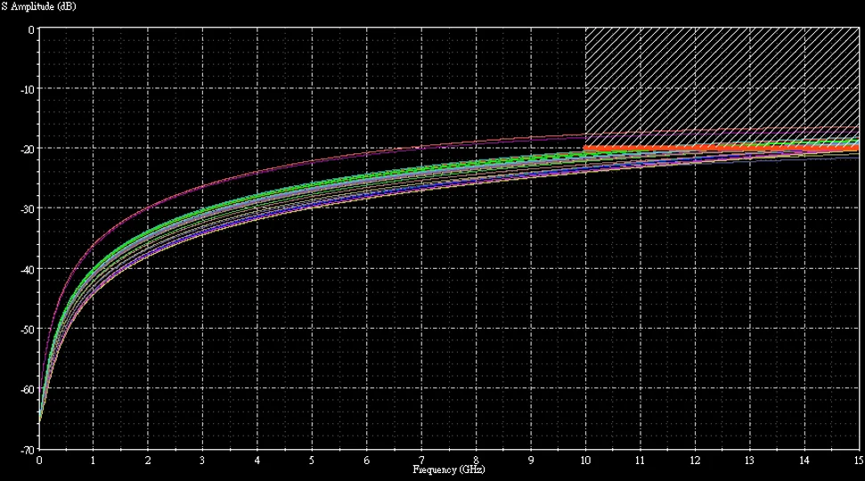
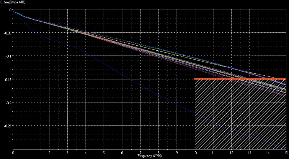
針對高頻高速應用進行專業 3S 參數模擬,深度分析 Insertion Loss 與 Return Loss。Professional 3S parameter simulation for high-frequency applications, with in-depth Insertion Loss and Return Loss analysis.
評估高功耗晶片在直流傳輸下的電壓降,確保電源網路設計具備足夠供電餘裕。Evaluates DC voltage drop in high-power chips, ensuring adequate margin in power network design.
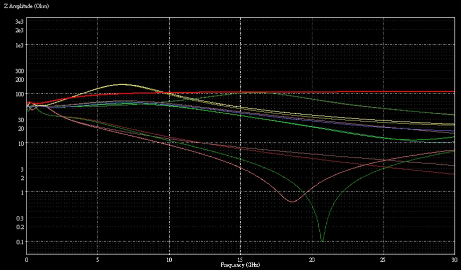
透過 PDN 阻抗與頻率響應模擬,降低電源雜訊,確保晶片運算時的電壓穩定性。PDN impedance and frequency-response simulation reduces power noise, ensuring voltage stability during chip operation.
RLCG 寄生參數等效電路模型RLCG Parasitic Equivalent Circuit Model
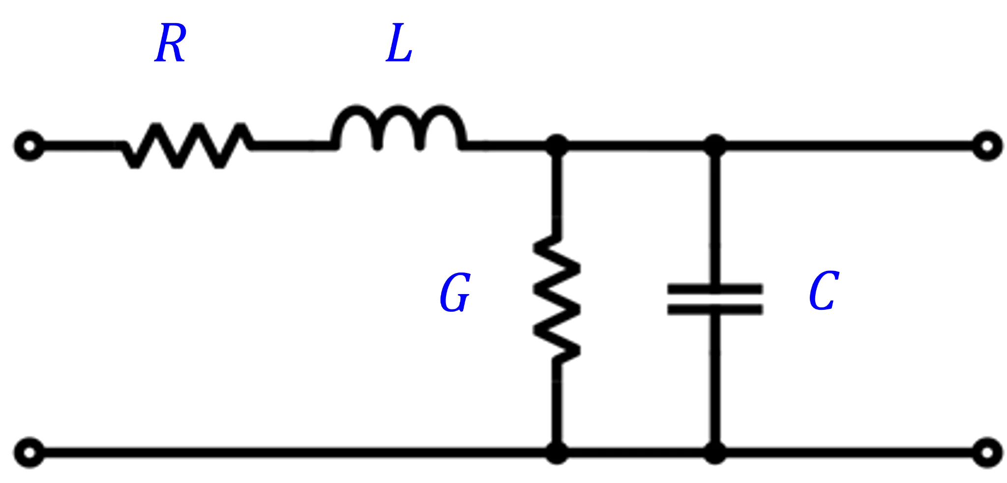
傳輸線路 RLCG 分散式等效電路模型:R(串聯電阻)、L(串聯電感)、G(並聯電導)、C(並聯電容)Distributed RLCG transmission-line model: R (series resistance), L (series inductance), G (shunt conductance), C (shunt capacitance)
高頻訊號與電源完整性分析曲線圖展示High-Frequency Signal & Power Integrity Analysis Charts
熱傳模擬Thermal Simulation
前瞻性封裝熱管理與動態熱模擬,解鎖高效能運算晶片散熱瓶頸Forward-looking package thermal management and dynamic thermal simulation, unlocking cooling bottlenecks for high-performance computing chips
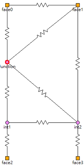
精確量測與計算晶片內部層間熱阻,為先進封裝材料選擇與散熱結構提供關鍵數據。Accurately measures and calculates interlayer thermal resistance, providing key data for advanced packaging material selection and heat-sink design.
提供符合國際標準的 Delphi 簡化熱模型(Delphi CTM),協助客戶進行系統級散熱架構快速評估。Internationally compliant Delphi Compact Thermal Models (Delphi CTM) enable rapid system-level thermal architecture assessment.
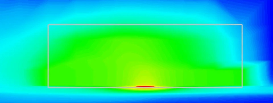
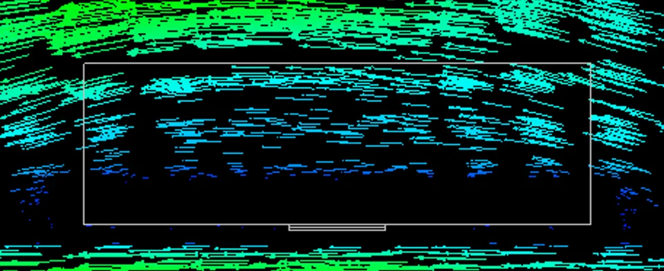
精準模擬自然對流與強制對流環境下散熱片與對流流體(Convection Velocity)的熱表現。Accurately simulates heat-sink and convection velocity thermal performance under natural and forced convection conditions.
針對高功耗晶片在時變功率(Time-Varying Power)運作下的動態熱分佈(Thermal Distribution)進行模擬,確保極端負載下的熱安全性。Simulates dynamic thermal distribution of high-power chips under time-varying power, ensuring thermal safety under extreme loads.